Bipolar Junction Transistor Theory
Transistors are current controlled solid-state devices that conduct current in proportion to an input current. The symbol for a transistor is shown in figure 1. The transistor on the left is called an "NPN" transistor and the transistor on the right is called a PNP transistor.
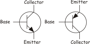
Figure 1) NPN and PNP Transistor Schematic Symbols
For an NPN transistor, current flowing "into" the base leg of the transistor results in a proportionally larger current to flow between the collector and the emitter. Conversely the current flowing "out" of the base of a PNP transistor allows a proportional current to flow between the emitter and the collector. This is shown in figure 2.
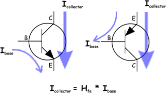
Figure 2) NPN and PNP Transistor Current Flow
The current between the base and the emitter is labeled Ibe, and the current between the collector and the emitter is Ice. The relationship between that currents is called the gain (or sometimes the Beta) of the transistor and it is labeled Hfe on the spec sheet. You'll notice something if you look closely at the current flows, they are reversed depending on the transistor type. So while the current Ice in an NPN transistor is positive, the current flows from the emitter to the collector in a PNP transistor so its Ice is written as a negative current. Similarly, Ibe on the NPN is positive and Ibe on the PNP is negative. This relationship becomes important when we use them to build a bridge.
The current proportion is Hfe, but the transistor doesn't actually generate current, what it does is "resist current less." What this means is that no current is flowing in the base, the transistor will resist all attempts to get current flowing between the collector and emitter. As the current in the base increases, that current multiplied by Hfe is allowed to flow between the collector and emitter, assuming such a current could flow.
The last bit is what confuses a number of people. Let's say you have a 9V battery connected to a 100 ohm resistor and then connected to and NPN transistor and finally to ground. Let's further assume that the beta (Hfe) of the transistor is 250. This is shown below in figure 3.
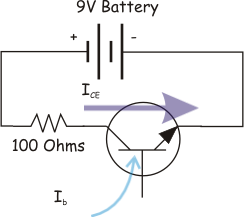
Figure 3) A simple circuit with a 9V battery and a resistor
What is the maximum current that can flow through the transistor? If we replace the transistor with a piece of wire, then using Ohm's law we can calculate the current flow to be 9/100 or .09 Amps (90 mA).
Now when the current is present, if it has a current of 2mA flowing into the base the maximum current the transistor will conduct is 2mA * Hfe, substituting in 250 for Hfe gives us 2 mA * 250 for a total of 500 mA.
And yet we know that if the transistor was a wire the most we would see is 90mA. So the actual answer is this "The amount of current that flows through the transistor is the lesser of the available current and Ibe*Hfe."
Generally if you apply enough base current that the maximum current possible will always flow, then the transistor is operating like a switch (rather than operating like an amplifier). In this mode, the transistor is said to be saturated.
One more thing and then we'll be done with the theory and into the practice. A BJT transistor will cause a drop in voltage between the collector and the emitter even when it is saturated (it isn't a perfect conductor). This voltage drop is called out in the data sheet as Vce(sat). Typically, this will be between .2 and 1 volts for silicon transistors. That means in an H-bridge configuration, if the top transistor has a .7v drop and the bottom transistor has a .7 volt drop, there will be a 1.4 volt drop in total. If you are using a 6v power supply, that will leave 4.5 volts for the motors. Ever wonder why a lot of toys use 4.5 volt motors? That's one reason! With a transistor H-bridge being driven by four batteries, the motors "see" 4.5 volts. What that means in our example above, is that if the transistor has a saturation voltage of .7 the max current that will flow when it is fully switched on it (9 - .7)/100 or 83mA.
There is also a voltage drop across the base-emitter junction. This is called out as Vbe in the data sheets. When you are calculating the current that will flow in the base, you must subtract this value from the total voltage drop before you compute the resistor value. For most (all?) silicon transistors this value is .7 volts.
The Vce(sat) voltage drop is also the source of power dissipation in the transistor. If you recall the formula for power is P = I * E, where I is current and E is voltage and the power is expressed in Watts. So given that the transistor has a saturation voltage between the collector and emitter of .7 volts, and you are conducting 3 amps through that transistor, this means the transistor is dissipating .7 * 3 or 2.1 watts. That is about the maximum a TO-220 case can dissipate before you have to put a heat sink on it. Keep that in mind when you are building h-bridges.
Next, BJT Transistor Selection ..
| Introduction | ||