Building a Test Bench
So we've got a parts list, a schematic, and you could just jump in and build this bridge to see if it will work. However, as this is both a theory and a practice tutorial I'll dive in a bit deeper than that.
 To understand how this bridge performs in
practice, I built one half of it on a piece of proto-board. I only had to
build "half" the circuit because the circuit is symmetrical, anything I can learn about
this half is equally applicable to the other half. The only thing this won't
tell me is what the behavior would be if the bridge switches from full forward to full
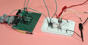
reverse in one go. The picture on the right shows the half bridge and a
Basic Stamp II board next to it on the left. The Basic Stamp is used as a test pattern
generator for my experiments.
To understand how this bridge performs in
practice, I built one half of it on a piece of proto-board. I only had to
build "half" the circuit because the circuit is symmetrical, anything I can learn about
this half is equally applicable to the other half. The only thing this won't
tell me is what the behavior would be if the bridge switches from full forward to full
reverse in one go. The picture on the right shows the half bridge and a
Basic Stamp II board next to it on the left. The Basic Stamp is used as a test pattern
generator for my experiments.
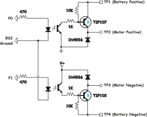
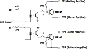 The
schematic of the test circuit is shown on the right. Inputs to this circuit
are P0 and P1 which reflect the names of the Basic Stamp 2 pins to which
those test points are connected. On the right side of the schematic are four
test points labeled TP1 through TP4 which correspond to the battery and
motor connections in the full schematic.
The
schematic of the test circuit is shown on the right. Inputs to this circuit
are P0 and P1 which reflect the names of the Basic Stamp 2 pins to which
those test points are connected. On the right side of the schematic are four
test points labeled TP1 through TP4 which correspond to the battery and
motor connections in the full schematic.
By building one half of the full h-bridge, I can turn on one low side (sink) transistor and one high side (source) transistor and then look at the waveforms and voltages under controlled conditions. The difference between this schematic and the one in the previous section is that half of the bridge is missing, and I've added independent control of the transistors. thus the FWD, REV, and ENA* lines aren't present.
For the static tests I have the Basic Stamp II simply turn on the transistors and leave them on. One additional piece of information gathered was that 470 ohm resistors work as do 560 ohm resistors. (560 turned out to be my final value that I used). If you don't have a Stamp or some other piece of equipment that generates signals you can simply connect the 1K resistors to TP1 and TP4 respectively. That will force the transistors on while you are doing the tests.
Static Tests
The first set of tests are static analysis of the transistor behavior. The three parameters I was most interested in were the voltage drop across the "source" transistor, the voltage drop across the "sink" transistor, and heat dissipation in the transistors. These tests are run with a voltmeter and an adjustable power supply. The datasheets include graphs of these parameters because they change for different currents. I thought I would pick three currents from which to take measurements of 10mA, 100mA, and 1000mA then plot the results. Note that the next step for current in a log scale would be 10 amps but the circuit is not rated for 10 amps. You could go to 2 amps (pretty much the limit without using heatsinks) or to 6 amps if the transistors had heatsinks installed.
Test #1 : Source side Voltage Drop
Purpose: The purpose of this test was to ascertain the voltage drop across the high side (source) transistor. The motor will see the battery voltage minus this voltage and the voltage drop across the sink transistor so knowing these values help define the lowest voltage that is practical with this bridge.
Description: A variable output bench top power supply is connected to TP1 and TP4. To create a load, a 4.7 ohm, 10 watt, power resistor is connected between TP2 and TP4. A digital voltmeter was connected between TP1 and TP2 and set to "DC Volts".
The power supply was turned on and its current output adjusted to 10 mA, a reading was taken on the voltmeter, then the current is increased to 100 mA and finally 1000 mA.
Test Results: The results of this test are collated in the table below. As the current through the transistor is changed from 10mA to 1000mA the voltage drop changes from a low of about .6 V to a high of about .9V. This change is plotted in the chart on the right side of the table.
| Current |
Measured Voltage Drop |
Chart |
|---|---|---|
| 10 mA |
0.602 V |
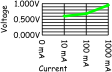 |
| 100 mA | 0.687 V | |
| 1000 mA | 0.950 V |
What this tells us is that as the current gets larger the transistor is less like a conductor and more like a resistor. The physics behind this change are due to the fact that silicon, unlike other metals, is transferring charge carriers (electrons and holes) through a crystal lattice. The larger the current, the more charge carriers are required, and the space in the lattice is finite. The result is that more charge carriers collide with the lattice generating heat, and the difference in charge going in vs. that going out is measured as a voltage drop. (recall that the voltage potential between two points is simply the difference in charge between those points)
Test #2 : Sink side Voltage Drop
Purpose: The purpose of this test was to ascertain the voltage drop across the low side (sink) transistor. The motor will see the battery voltage minus this voltage and the voltage drop across the source transistor so knowing these values help define the lowest voltage that is practical with this bridge.
Description: A variable output bench top power supply is connected to TP1 and TP4. To create a load, a 4.7 ohm, 10 watt, power resistor is connected between TP1 and TP3. A digital voltmeter was connected between TP3 and TP4 and set to "DC Volts".
The power supply was turned on and its current output adjusted to 10 mA, a reading was taken on the voltmeter, then the current is increased to 100 mA and finally 1000 mA.
Test Results: Again I've collected the results into a table below. To bring this back to a global point about this web site, there is a page in my "physical" robotics notebook where I hand drew a box with 10, 100, and 1000 in the left hand side, then as I got measurements I wrote them to the right. Around the box I identified these results as being "Sink Experiment #2" and the date. I can go back later and refer to the notebook pages I created during this project and easily re-create my experiment or refresh my self on the results of that experiment.
| Current |
Measured Voltage Drop |
Chart |
|---|---|---|
| 10 mA | 0.576 V | 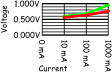 |
| 100 mA | 0.637 V | |
| 1000 mA | 0.763 V |
When that transistor is "off" the voltage rises to the input voltage of 10V, when the transistor is "on" it drops to the difference between the voltage on the low side collector and the battery minus connection. Again its in the neighborhood of .75V. In the chart I've shown the sink voltage drop in red and the source voltage drop in green.
Test #3 : Thermal Constants for the TIP107 and TIP102
Purpose: The purpose of this test was to ascertain what the current capacity for the bridge will be when it does not have heat sinks on the transistors. This value will vary with ambient conditions but this test attempts to establish a baseline which will help us decide if we must put heat sinks on the transistors in general or only in special cases.
![]() Description: The half
bridge is set up with a variable power supply attached to the "Battery
Positive" and "Battery Negative" test points. A resistor is
connected between the sink resistor and "Battery Positive" which will
provide a regulated load. The transistor was instrumented with a type K
thermocouple that was attached to my Fluke meter. The transistor with the
thermocouple attached is shown in the picture to the right. I took great care to put an insulator
between the transistor tab and the bolt to prevent the bolt from becoming
part of the thermal mass being measured.
Description: The half
bridge is set up with a variable power supply attached to the "Battery
Positive" and "Battery Negative" test points. A resistor is
connected between the sink resistor and "Battery Positive" which will
provide a regulated load. The transistor was instrumented with a type K
thermocouple that was attached to my Fluke meter. The transistor with the
thermocouple attached is shown in the picture to the right. I took great care to put an insulator
between the transistor tab and the bolt to prevent the bolt from becoming
part of the thermal mass being measured.
Under three loads, 10mA, 100mA, and 1000mA, the temperature is measured until it stabilizes. Note that for both the 100mA and 1000mA tests the voltage is constantly adjusted to keep the current level the same. This is because BJT transistors have a 'negative' temperature coefficient, when they get hotter they conduct more current. This can lead to thermal runaway if the supply and load can conduct higher currents. In addition to the temperature measurements, the voltage drop is measured across the transistor.
The power being dissipated by the transistor will be equal to the current multiplied by the Vce voltage. The Rtheta(ca) value (case to ambient) will be the difference in temperature (from the initial reading) divided by the dissipation in watts giving a value in °C/Watt.
Initially I used a non-contact thermometer to measure the temperature of the transistor. I have the IR-101 from La Crosse Technology. This can measure either Centigrade or Fahrenheit and also maintains min/max measurements. The challenge was reading the transistor and not the resistor (which gets really hot), and the emissivity of the transistor tab doesn't give good readings (accurate to 2.5 degrees).
Test Results: Initial measurements put the TO-220 case at 20.1 °C, The temperature measured at each current level is recorded in the table below. The value for Rtheta(ja) is computed for each measurement point.
| Current |
Voltage Drop |
Power Dissipation |
Measured Temperature |
Computed Rtheta(ja) |
|---|---|---|---|---|
| 0 mA | N/A | N/A | 20.1 °C | N/A |
| 10 mA | 0,576 V | .006 W | 20.8 °C (+ 0.7 °C) | 116.7 °C/W |
| 100 mA | 0.637 V | .064 W | 27.6 °C (+ 7.5 °C) | 117.2 °C/W |
| 1000 mA | 0.717 V | .717 W | 67.7 °C (+ 47.6 °C) | 66.4 °C/W |
The interesting thing to me was that the temperature coefficient got a lot smaller when the current was greater. The data sheet for the TO-220 specs a value of 62 °C/W which is pretty close to the last measurement. When I thought about it I realized that this effect stems from the "thermal resistance" of the ambient air. The energy transfer is proportional to the difference in temperature, as the temperature difference goes up, more heat is pushed "into" the air more quickly. Further, a convection current is established as the air next to the transistor heats up and rises allowing cooler air to replace it. By blowing on the transistor I could easily bring the temperature down to 60 °C.
Static Tests Summary
The transistors have a voltage drop that is between .7 and 1V under load. Its "between" these numbers because as the current through the transistor increases so does the voltage drop. Given that the torque output of a motor is proportional to its current, we must insure that the voltage the motor "sees" will be sufficient to get the maximum torque. Referring to the Mabuchi RS-280RA/SA data sheet, we see that the 7.2V model (RS-280RA-2485) delivers maximum torque (220g*cm) at 6.6Amps of current when it is stalled. To get this much current requires a full 7.2V of voltage potential so the motor, so allowing for 2V of voltage drop means the input batteries should probably be 9.6V NiCd's. However, the nominal power this motor consumes is 1.18A when pushing 33.3 g·cm of torque (at 14,300 RPM). If you've geared this down 10:1 your looking at 333 g·cm of torque at 1430 RPM. A "fast" robot can move at 10'/second so to travel at 1430 RPM that is 24 revolutions per second, and to cover 120" each revolution would have to move the robot 5". Dividing 5 by π gives a diameter of 1.6" (or a radius of 2 cm). So torque delivered by the motor to the rim of a wheel 4cm in diameter behind a 10:1 gearbox will be about 150 gm. Two of these motors would provide 300gm of torque to the ground while cruising. Startup torque (to accelerate from a dead stop) 1.1Kg per wheel or 2.2Kg for two wheels. Basically enough to accelerate a 3Kg Sumo robot at nearly 1G if the traction held.
The bottom line is that for a robot that weighs 5 to 16 lbs (2 - 8 Kg) a pair of these bridges driving a pair of the Mabuchi motors with 10:1 gearboxes would make for a pretty peppy robot. The closer you got to an 8Kg robot the more likely you would need to add heatsinks to the bridge (more often pulling more than 1.5A) and for robots of 2 or 3 Kg the bridge as is will be fine.
Dynamic Tests
 In order to investigate how this
bridge responds when it is driving an inductive load, a slight change was made. The modification consists of
adding two fast recovery silicon rectifiers. I've used a pair of
1N4936 diodes which are a bit of
overkill with a 400V reverse voltage limit but they are inexpensive.
Further, having a
better margin for error is always good. The updated schematic is shown to
the right. You will recall these diodes are shown as "optional" in the full
H-bridge circuit. The newly added diodes are installed in place of the sink
transistor in the lower left of the bridge and the source transistor in the upper right
area.
In order to investigate how this
bridge responds when it is driving an inductive load, a slight change was made. The modification consists of
adding two fast recovery silicon rectifiers. I've used a pair of
1N4936 diodes which are a bit of
overkill with a 400V reverse voltage limit but they are inexpensive.
Further, having a
better margin for error is always good. The updated schematic is shown to
the right. You will recall these diodes are shown as "optional" in the full
H-bridge circuit. The newly added diodes are installed in place of the sink
transistor in the lower left of the bridge and the source transistor in the upper right
area.
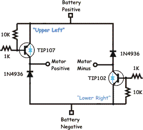 The two transistors are sporting
light blue diode symbols to remind you that the TIP 102 and TIP 107
transistors have a built in freewheeling diode. If you re-arrange the
circuit it would like like the schematic shown on the left.
The two transistors are sporting
light blue diode symbols to remind you that the TIP 102 and TIP 107
transistors have a built in freewheeling diode. If you re-arrange the
circuit it would like like the schematic shown on the left.
With The test circuit I still can't reverse the motor's direction, but I can change its speed. As the h-bridge circuit is symmetric, I can use this circuit to study the behavior of the bridge when it is driving a motor with a DC signal and a PWM signal.
To generate control signals for the dynamic tests I've used a test pattern generator. My "test pattern generator" in this case is a Parallax Basic Stamp II that is running The following simple program:
|
'{STAMP BS2} ' ' A Simple Test Program to run my test bench setup ' DIRA = 3 ' Set up pins 0 and 1 as outputs OUTA = 0 ' Initial state, transistors off. Loop: OUTA = StateA ' Transistor state set to "A" PULSOUT 2,100 ' A finer grain delay than PAUSE OUTA = StateB ' Transistor state set to "B" PULSOUT 2,100 ' A finer grain delay than PAUSE GOTO Loop END |
When pin P0 on the BS2 is set to be an output and "high" (logic 1 level) it puts 5V on the P0 input of our test circuit. This causes the opto-isolator's LED to illuminate and that causes the transistor to turn "on." The opto-isolator's transistor connects the base of the TIP107 transistor to ground and that turns that transistor on. Similarly when P1 is made "1" by the BS2, it turns on the sink transistor using a similar mechanism. As you can see in the program the transistors are changed from state "A" to state "B" and back again, but neither "A" nor "B" are specified. That is because there are many ways you might want to drive your bridge.
There are two primary ways of driving an H-bridge, one is called "sign magnitude" and "locked anti-phase." A good description of the difference can be found on Larry Barrello's site (see the motion control pages). I tend to use sign-magnitude as it does not depend on specific timing relationships between the source and sink transistors. Specifically, transistors do not turn on and off at the same speed. The locked anti-phase technique of motor control requires that the bridge switch directions "instantly" so that there isn't an opportunity for both the source and sink transistors of the same side of the bridge, being active at the same time. Bridges that support locked anti-phase will have logic inside the bridge to specifically delay the turn on of the sink our source to match the turn off time of that element's counterpart.
Test #1 : Contributions of Resistance and Inductance
Purpose: A permanent magnet DC motor can be modeled by three components in series;, a resistor, an inductor, and a voltage source. Resistance is due to the wire resistance of the motor's windings, inductance is due to the geometry of those windings, and the voltage source arises from the interaction between the permanent magnets in the motor and the windings. The purpose of this test was to look at the waveform of the voltage across the motor when the bridge was operating and to determine how each of these three components contribute to that waveform.
Description: An oscilloscope is set up to take a differential measurement between TP2 and TP3. This is accomplished by hooking channel 1 to TP2, channel 2 to TP3 and then using the "add" and "invert" buttons to create a composite output. The result can be expressed mathematically as "CH1 + (- CH2)." As they are both measuring a waveform with respect too a common ground, any difference in the two waveforms will show up in the composite waveform. Three sub-tests tests are run, one with a resistor connected between TP2 and TP3, one with an inductor connected between TP2 and TP3, and one with a motor connected between TP2 and TP3. Each test generated a waveform and each waveform is photographed and recorded. The Basic Stamp II is connected to P0 and P1 and the test program is run. StateA was set to 3 (both transistors on) and StateB was set to 0 (both transistors off).
Test Results: The results of this test were fairly interesting to me, they gave me a good picture of what the components of the waveform observed were.
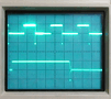
| The first sub-test used a resistor. The results were photographed and are shown in the scope trace to the right. There isn't a whole lot of surprise here, the output is an amplified version of the square wave that the BS2 is generating. The scope was set to 10V per division so the resulting square wave is 10V peak to peak. The bottom trace is an expanded view of the upper trace. |
|
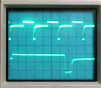
| The second sub-test used an inductor. The photograph of those results is shown on the right. Again the scope is set to a resolution of 10V per division, but this time when the transistors turn off there is a -10V "spike". There are two things about the spike that are interesting, the first is that it is nearly exactly -10V, and the second is that it is quite short. More about that in a bit. |
|
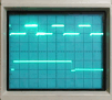
| The final sub-test used a permanent magnet DC motor. Again the results are in the photograph to the right. This one has the square wave from the resistor, the spike from the inductor, and now a moderately curving up tick to 5V and periodic glitches to 10V (not visible in this image sorry.) |
|
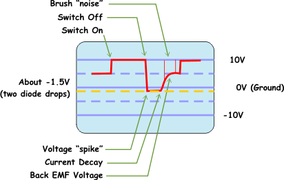
I've re-drawn the final waveform and annotated the results, they are shown below.
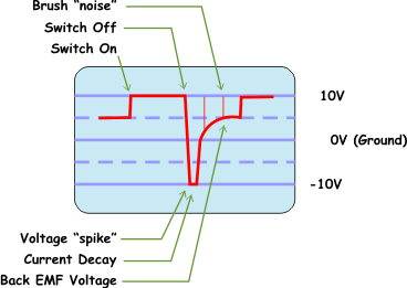
Starting from the left of the waveform and moving to the right. The voltage across the motor jumps to 10V when the two transistors are switched "on." This part of the wave form comes from the resistive nature of the motor, if it were a perfect conductor then the voltage drop across the motor would be zero according to Ohm's law. Then when they are switched "off" the voltage makes an apparent reversal (more on this after test #2) and the voltage stays at -10V for a short period of time while the current in the motor's windings decays. This component is contributed by the inductance of the motor as it matches exactly the waveform of the inductor only subtest. Finally the motor returns to zero but then continues to 5V. This is the contribution of the "generator effect" or back EMF voltage of the motor. Because the motor has mass and it is still spinning, its inertia causes it to continue to rotate. This rotation moves the windings past the permanent magnets and the motor becomes a generator.
The interesting thing for me was the spikes in the EMF component. After thinking about it for a while I realized that a permanent magnet DC motor has brushes that reverse the polarity of the windings when the stator is turning. When those brushes switch, they disconnect the motor winding resulting in an inductive spike as well. That spike can be controlled (but not eliminated) by putting a capacitor across the motor terminals.
Test #2 : Which to switch, High, Low, or Both
Purpose: One of the arguments that you hear in robot groups and on line is how sign magnitude PWM should be implemented. Specifically, should you switch both the high side and low side transistors? Or just the high side? or just the low side? The argument goes that switching the high side eliminates spikes or switching them both increases efficiency, and on and on. This test was designed to try all three options (high, low, and both) and to analyze the results.
Description: An oscilloscope is set up to take a differential measurement between TP2 and TP3. This is accomplished by hooking channel 1 to TP2, channel 2 to TP3 and then using the "add" and "invert" buttons to create a composite output. The result can be expressed mathematically as "CH1 + (- CH2)." As they are both measuring a waveform with respect too a common ground, any difference in the two waveforms will show up in the composite waveform. Three sub-tests tests are run; One by switching off both transistors, one by switching off the sink (low) transistor, and one by switching off the source (high) transistor. Each test generated a waveform and each waveform is photographed and recorded. The Basic Stamp II is connected to P0 and P1 and the test program is run. The following values are used for variable StateA and StateB.
| Sub-test | StateA | StateB |
|---|---|---|
| Both Transistors switched | 0x03 | 0x00 |
| Sink Transistor (low side) switched | 0x03 | 0x02 |
| Source Transistor (high side) switched | 0x03 | 0x01 |
Test Results: The results are collected in the table below.
| Resistor | Inductor | Motor | Description |
|---|---|---|---|
 |
 |
 |
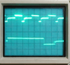
This is the series of tests where I switch both the source and the sink transistor at the same time. The interesting thing to note is the larger spike when the bridge is switched "off" |
|
 |
 |
This is the series of tests where I switched off the "sink" transistor only. This leaves the source transistor on during the entire time. In these sequences you can see the inductive kick from the inductor is apparently "missing" (it isn't however...) |
As it turned out the last two sub-tests produced identical results so only one set of results is not shown. It was interesting to me that there were only two unique results out of three possible tests. To understand that I needed to understand what was going on with the motor inductance.
Remember in test #1 above where the voltage across the inductor appears to go negative? Well how could that be given that an inductor resists a change in current? The answer is that it isn't actually negative. Remember that the scope probes are measuring the voltage across the inductor, when there is a current flowing in the inductor a magnetic field develops around it (this is its way of storing energy). When the current stops because a switch is thrown open, the collapsing magnetic field of the inductor continues to push current through. But a current, is really just charge in motion. The charge in question has no where to go. So that charge "builds up" on the end of the inductor. And because voltage is simply the difference in charge, the voltage potential between the ends the inductor begins to rise. Its important to note that the charge came from the other end of the inductor, so this voltage potential is really relative to that end. The relationship between the voltage rise relative to the other end of the inductor means that some path needs to be found to return those electrons to the other side. If you somehow managed to eject the motor the dielectric constant of the air would break down as the voltage potential rose and you would get an arc as a circuit was created with ionized air to the other terminal! Fortunately, the h-bridge has other paths.
When both transistors are switched off, the voltage rises until it begins to be higher than than the battery voltage. At that point there is a circuit path backwards through the battery to the other end of the inductor. This, in effect, dumps charge back into the battery. (not a lot, just the amount of charge stored as flux in the magnetic field of the inductor).
When only one transistor is switched off the story is completely different. Now as the potential rises it eventually passes the forward voltage of the 1N4963 free wheeling diode. At that point it sees the "conducting" transistor on the other side of the bridge, Once it is higher than that transistor's voltage drop the rest can simply pass through to the other end of the inductor. That wave form looks like the one below.
Now instead of seeing "-10V" the inductor sees something like -1.5 volts. Why not zero volts? Because the current is traveling through the freewheeling diode and the transistor that is still on, consequently there are two voltage drops between it and the other end of the inductor. When summed together those drops add up to about 1.5 volts.
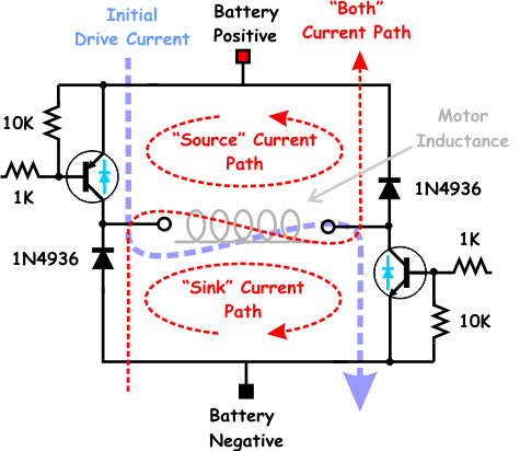
Now I can draw a picture of the test circuit and all the various current paths. This is shown in the schematic below. The blue dashed line represents the current flow before the PWM wave form is switched "off." The red dashed lines represent the path of the decay current out of the inductor depending on which option you use for switching off the transistors.
One of the members of the HBRC asked, "But if you switch just one transistor, isn't the other one shorting the motor and causing it to brake?" This is an excellent question and one that I might have answered incorrectly had I not been through this analysis.
When you short a rotating motor the voltage that the motor is generating is opposite to the voltage that you would need to turn the motor the other way (hence the term 'back' EMF). If you look at the scope traces and refer to the schematic above, you will note that for our test cases the back EMF is "positive" with respect to our measuring probes. That means that the voltage generated creates a higher potential on the left terminal of the motor than the right terminal. If you create a connection between the left and right terminal of the motor, the current will flow from the left terminal, into the right terminal and try to drive the motor in the other direction. (Just as if we had switched the bridge the other way) But this current in our circuit is impeded by the freewheeling diode on the right terminal that is reverse biased relative to that voltage. Hence, no braking action occurs. If on the other hand you turn on the upper right transistor while the upper left transistor is on, there is nothing to impede the flow and the motor slows down rapidly.
Next: Using the H-Bridge
| Implementing an H-bridge | ||